
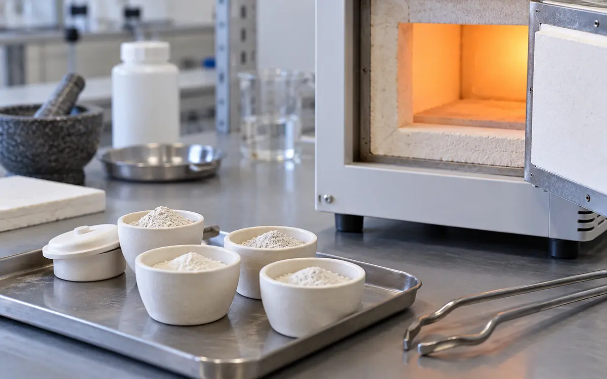
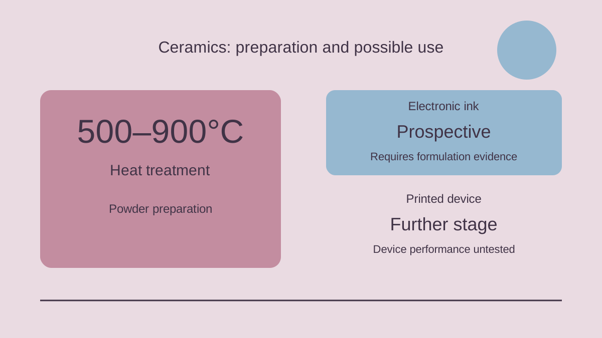
Researchers at the Moscow Institute of Physics and Technology in Russia have developed a method for producing nanoscale ceramics intended for future electronic inks. Interfax reported the work on 12 February 2025. The material is based on indium, gallium and zinc compounds. According to the university, varying heat treatment between 500 and 900°C allows different degrees of crystallinity while retaining small particles. Researcher Gleb Zirnik links that objective to the requirements of inks for printing electronic devices.
What the material study examines
The research abstract identifies the ceramic as InGaZnO4 and describes a metal-nitrate-glycol gel decomposition method. It reports X-ray diffraction studies of particle growth, together with electron microscopy and elemental analysis. The latter indicated a uniform distribution of the constituent elements. These observations concern the prepared material; they do not constitute a performance test of a finished printed transistor.
The distinction matters because a material and a device answer different practical questions. Producing a candidate powder establishes a starting point for development. It does not by itself establish how a printable formulation behaves during storage, deposition or operation in an electronic component.
Separate stages of the proposed application
- The reported research concerns obtaining and characterising ceramic material.
- The proposed next application is an ink based on that material.
- A functioning printed device would be a further result requiring its own evidence.
Keeping those stages separate makes the announcement more informative. It allows the measured properties to be discussed without presenting a possible application as an existing manufacturing product. In particular, a temperature used to prepare powder should not automatically be read as the temperature at which a future flexible device would be printed.
Why the next comparison matters
For an eventual ink, a useful assessment would connect the preparation conditions to the properties required by a specific printing task. A smaller particle size alone would not settle every question about the formulation. The relevant comparison would need to explain which property is improved and how that improvement carries through to the intended application.
The present result is therefore best understood as a materials-development contribution. It creates a route to investigate further, while leaving the performance of a complete ink and device to subsequent work.
Sources: Interfax; research paper and abstract.
Sources: Интерфакс; SPbU research portal / Ceramics International abstract; MIPT representatives via CNews, supplementary contemporary statement.




Leave a comment